
How is power consumption optimized in semiconductor memory types?
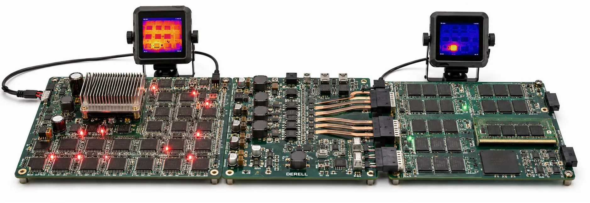
Make each memory access count—and let idle hardware rest
Memory energy falls when the technology fits the workload, unnecessary accesses disappear and idle periods use suitable power modes. There is no universal setting for every device. Working data in RAM and a permanent event log have different requirements. Start with the application, required retention and response time.
Separate active, standby and data-retention consumption. Reads and writes cost energy, powered circuits draw leakage and standby current, and DRAM also needs refresh. A single current specification is not enough to predict system battery life.
What changes with the memory technology?
| Memory | Useful approach | Constraint |
|---|---|---|
| DRAM | Use supported power-down or self-refresh modes and reduce unnecessary traffic. | Self-refresh needs power to retain data. Refresh timing must stay within the manufacturer's limits. |
| SRAM | Use supported retention modes; switch off banks whose contents are no longer needed. | No periodic refresh, but retention still requires appropriate power. Disabled banks may lose their contents. |
| Flash / EEPROM | Avoid redundant writes, use supported page/block operations efficiently and enter suitable sleep modes. | Finish programming or erasing before removing power. Operation rules and wake-up delays are device-specific. |
| FRAM | Consider low write energy for frequently updated small records. | Compare actual active and standby current, capacity and interface requirements. |
| MRAM | Use nonvolatile retention to explore supported power-off arrangements. | Nonvolatile storage does not automatically mean the lowest energy for every workload. |
The DRAM–SRAM distinction matters: DRAM cells need refresh, while SRAM does not use that periodic process. NVRAM is an umbrella term rather than one cell technology; FRAM, MRAM and backed-up memory can have very different power behaviour. NOR and NAND Flash also need separate treatment because their access, erase and programming arrangements differ.
Remove work before changing clock speeds
Reduce repeated reads, unnecessary copies and redundant writes. Caching and good data locality can cut external-memory traffic. Interrupts can replace continuous status polling where appropriate, and DMA may let a processor rest during supported transfers. DMA still accesses memory, though: verify the saving with the actual workload.
In a data logger, buffering samples and writing them in suitable groups can reduce transaction overhead. The trade-off is that records waiting in a volatile buffer are not yet persistent. Decide how much uncommitted data is acceptable when configuring the recording schedule. Follow the device's page-program and sector-erase rules for Flash, or its supported write arrangement for EEPROM.
Size the memory for the real job. Excess capacity can add chips, supply loads or standby consumption, but power does not always scale directly with capacity. Balance capacity and speed against data throughput and the required logging capacity. Updating a small counter frequently is a different workload from keeping a large historical archive.
A simple duty-cycle calculation
Illustrative assumptions: at a constant supply voltage, a memory subsystem draws 10 mA for 1 ms and 10 µA for the remaining 99 ms of each 100 ms cycle. Ignoring extra transition energy for this first calculation:
Iaverage = (10 mA × 1 ms + 0.01 mA × 99 ms) / 100 ms = 0.1099 mA ≈ 110 µA
These are teaching values, not product specifications. A real budget must include sleep entry, wake-up, reinitialisation and state restoration. Deep sleep may not pay off during a very short idle interval. With multiple supply rails, compare power and energy rather than simply adding or comparing current figures.
Voltage and frequency are only part of the budget
CMOS switching power is approximately related to Pdynamic ≈ α × C × V² × f. Supported lower-voltage operation and reduced switching activity can therefore help. This relationship does not describe every source of memory power. Keep voltage, clock rate and access timing within the data sheet. A slower clock can extend task duration, so lower instantaneous power does not necessarily produce the expected reduction in energy per task.
Include the surrounding circuitry. Regulator quiescent current, address/data-line switching, pull-up resistors and interface termination can affect the result. A powered-down memory also needs an interface arrangement that prevents unintended current through its signal pins. Choose battery and supply options for the complete system, not just the memory chip.
Apply the changes in a practical order
For an industrial IoT sensor, measure the operating cycle first. Then remove unnecessary writes, use supported power modes and compare suitable memory parts. On a finished PLC or recorder, memory voltage and refresh controls usually belong to the hardware design. Work through the manufacturer's recording interval, sleep and power-management options. Choose the final arrangement using energy per task and reliable data retention together.
Technical references: Micron DRAM power calculators · Infineon F-RAM power modes · Microchip Flash power management